Äîêóìåíòàöèÿ è îïèñàíèÿ www.docs.chipfind.ru
1
LTC1346A
10Mbps DCE/DTE
V.35 Transceiver
S
FEATURE
D
U
ESCRIPTIO
s
Single Chip Provides Complete Differential Signal
Interface for V.35 Port
s
Drivers and Receivers Will Withstand Repeated
±
10kV ESD Pulses
s
10Mbaud Transmission Rate
s
Meets CCITT V.35 Specification
s
Operates from
±
5V Supplies
s
Shutdown Mode Reduces I
CC
to Below 1
µ
A
s
Selectable Transmitter and Receiver Configurations
s
Independent Driver/Receiver Enables
s
Transmitter Maintains High Impedance When
Disabled, Shut Down or with Power Off
s
Transmitters Are Short-Circuit Protected
The LTC
®
1346A is a single chip transceiver that provides
the differential clock and data signals for a V.35 interface
from
±
5V supplies. Combined with an external resistor
termination network and an LT
®
1134A RS232 transceiver
for the control signals, the LTC1346A forms a complete low
power DTE or DCE V.35 interface port.
The LTC1346A features three current output differential
transmitters and three differential receivers. The trans-
ceiver can be configured for DTE or DCE operation or
shutdown using three Select pins. In the shutdown mode,
the supply current is reduced to below 1
µ
A.
The LTC1346A transceiver operates up to 10Mbaud. All
transmitters feature short-circuit protection. Both the trans-
mitter outputs and the receiver outputs can be forced into
a high impedance state. The transmitter outputs and re-
ceiver inputs feature
±
10kV ESD protection.
s
Modems
s
Telecommunications
s
Data Routers
U
S
A
O
PPLICATI
, LTC and LT are registered trademarks of Linear Technology Corporation.
V
CC1
5V
2
1
4
1
2
24
23
12
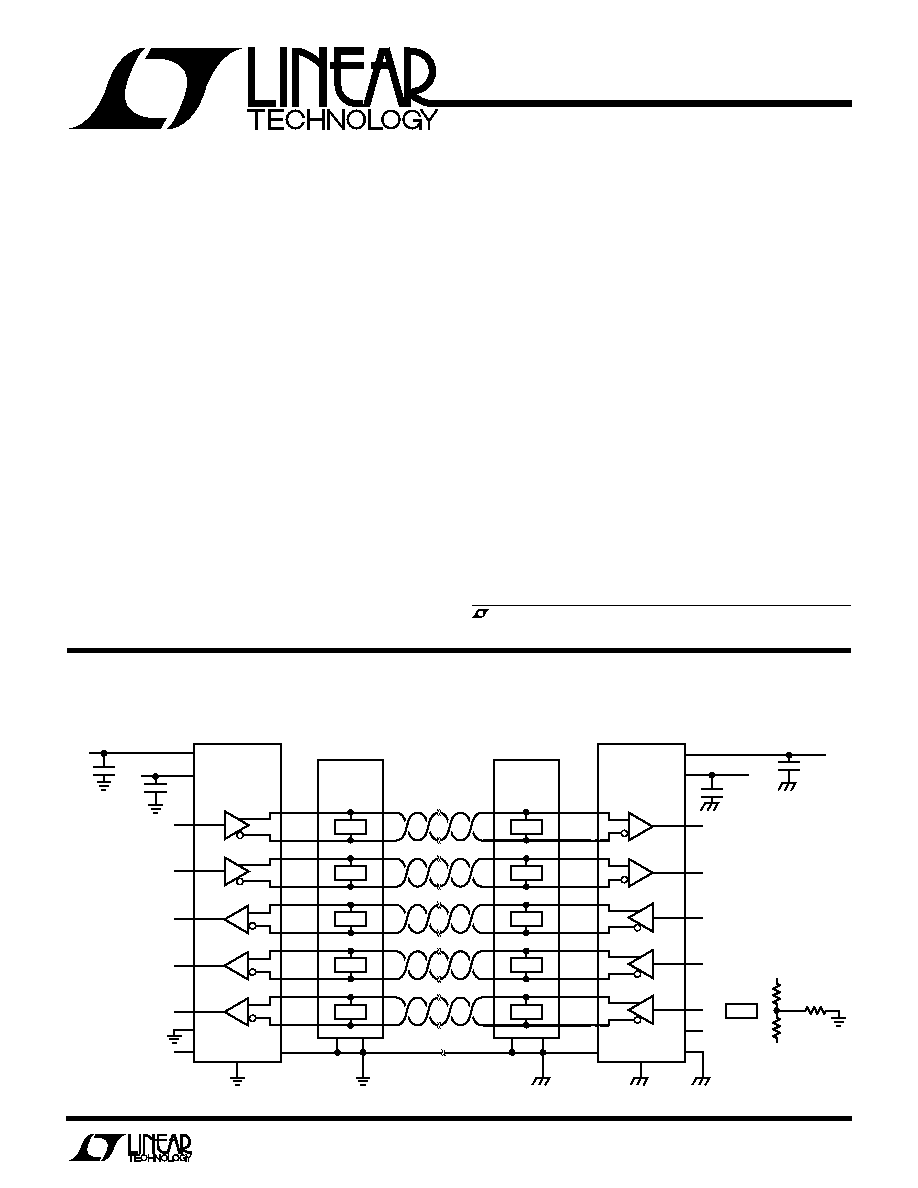
DTE
DCE
10
11
16
15
0.1
µ
F
DX
LTC1346A
LTC1346A
BI
627T500/1250
BI
627T500/1250
BI TECHNOLOGIES
627T500/1250 (SOIC)
V
CC2
5V
0.1
µ
F
2
RX
T
TXD (103)
SCTE (113)
TXC (114)
RXC (115)
RXD (104)
GND (102)
T
5
3
4
22
21
10
11
9
14
13
DX
RX
T
T
9
14
13
18
17
1
4
2
24
23
T
T
10
12
11
16
15
12
7
8
3
5
4
22
21
T
T
7
8
11
8
7
10
9
14
13
3
5
6
8
7
V
CC2
V
CC1
6
20
19
3
T
T
RX
RX
RX
12
LTC1346 · TA01
DX
DX
DX
50
=
125
T
50
+
V
EE2
5V
0.1
µ
F
1
+
+
V
EE1
5V
0.1
µ
F
+
Clock and Data Signals for V.35 Interface
TYPICAL APPLICATIO
N
U

2
LTC1346A
Consult factory for Military grade parts.
A
U
G
W
A
W
U
W
A
R
BSOLUTE
XI
TI
S
W
U
U
PACKAGE/ORDER I FOR ATIO
T
JMAX
= 150
°
C,
JA
= 85
°
C/W
(Note 1)
Supply Voltage
V
CC
.................................................................... 6.5V
V
EE
................................................................... 6.5V
Input Voltage
Transmitters ........................... 0.3V to (V
CC
+ 0.3V)
Receivers ............................................... 18V to 18V
S0, S1, S2 ............................... 0.3V to (V
CC
+ 0.3V)
Output Voltage
Transmitters .......................................... 18V to 18V
Receivers ................................ 0.3V to (V
CC
+ 0.3V)
Short-Circuit Duration
Transmitter Output ..................................... Indefinite
Receiver Output .......................................... Indefinite
Operating Temperature Range
LTC1346AC ............................................ 0
°
C to 70
°
C
LTC1346AI ........................................ 40
°
C to 85
°
C
Storage Temperature Range ................ 65
°
C to 150
°
C
Lead Temperature (Soldering, 10 sec) ................. 300
°
C
1
2
3
4
5
6
7
8
9
10
11
12
24
23
22
21
20
19
18
17
16
15
14
13
V
EE
V
CC
GND
T1
T2
T3
S1
S2
R3
R2
R1
S0
Y1
Z1
Y2
Z2
Y3
Z3
A3
B3
A2
B2
A1
B1
SW PACKAGE
24-LEAD PLASTIC SO WIDE
TOP VIEW
ORDER PART
NUMBER
SYMBOL
PARAMETER
CONDITIONS
MIN
TYP
MAX
UNITS
V
OD
Transmitter Differential Output Voltage
4V
V
OS
4V (Figure 1)
q
0.44
0.55
0.66
V
V
OC
Transmitter Common Mode Output Voltage
V
OS
= 0V (Figure 1)
q
0.6
0
0.6
V
I
OH
Transmitter Output High Current
V
Y, Z
= 0V
q
12.6
11
9.4
mA
I
OL
Transmitter Output Low Current
V
Y, Z
= 0V
q
9.4
11
12.6
mA
I
OZ
Transmitter Output Leakage Current
5V
V
Y, Z
5V, S1 = S2 = 0V
±
1
±
20
µ
A
q
±
100
µ
A
R
O
Transmitter Output Impedance
2V
V
Y, Z
2V
100
k
V
TH
Differential Receiver Input Threshold Voltage
7V
(V
A
+ V
B
)/2
12V
q
25
200
mV
V
TH
Receiver Input Hysterisis
7V
(V
A
+ V
B
)/2
12V
50
mV
I
IN
Receiver Input Current (A, B)
7V
V
A, B
12V
q
0.7
mA
R
IN
Receiver Input Impedance
7V
V
A, B
12V
q
17.5
30
k
V
OH
Receiver Output High Voltage
I
O
= 4mA, V
A, B
= 0.2V
q
3
4.5
V
V
OL
Receiver Output Low Voltage
I
O
= 4mA, V
A, B
= 0.2V
q
0.2
0.4
V
I
OSR
Receiver Output Short-Circuit Current
0V
V
O
V
CC
q
7
40
85
mA
I
OZR
Receiver Three-State Output Current
S0 = V
CC
, 0V
V
O
V
CC
q
±
10
µ
A
V
IH
Logic Input High Voltage
T, S0, S1, S2
q
2
V
V
IL
Logic Input Low Voltage
T, S0, S1, S2
q
0.8
V
I
IN
Logic Input Current
T, S0, S1, S2
q
±
10
µ
A
V
CC
= 5V
±
5%, V
EE
= 5V
±
5% (Note 2)
DC ELECTRICAL CHARACTERISTICS
LTC1346ACSW
LTC1346AISW
3
LTC1346A
SYMBOL
PARAMETER
CONDITIONS
MIN
TYP
MAX
UNITS
I
CC
V
CC
Supply Current
V
OS
= 0V, S0 = Low, S1 = S2 = High (Figure 1)
q
40
50
mA
No Load, S0 = Low, S1 = S2 = High
q
6
9
mA
Shutdown, S0 = V
CC
,
S1 = S2 = 0V
q
0.1
100
µ
A
I
EE
V
EE
Supply Current
V
OS
= 0V, S0 = Low, S1 = S2 = High (Figure 1)
q
40
50
mA
No Load, S0 = Low, S1 = S2 = High
q
6
9
mA
Shutdown, S0 = V
CC
,
S1 = S2 = 0V
q
0.1
100
µ
A
t
r
, t
f
Transmitter Rise or Fall Time
V
OS
= 0V (Figures 1, 3)
q
7
40
ns
t
PLH
Transmitter Input to Output
V
OS
= 0V (Figures 1, 3)
q
25
70
ns
t
PHL
Transmitter Input to Output
V
OS
= 0V (Figures 1, 3)
q
30
70
ns
t
SKEW
Transmitter Output to Output
V
OS
= 0V (Figures 1, 3)
5
ns
t
PLH
Receiver Input to Output
V
OS
= 0V (Figures 1, 4)
q
50
100
ns
t
PHL
Receiver Input to Output
V
OS
= 0V (Figures 1, 4)
q
55
100
ns
t
SKEW
Differential Receiver Skew,
t
PLH
t
PHL
V
OS
= 0V (Figures 1, 4)
5
ns
t
ZL
Receiver Enable to Output Low (Active Mode)
C
L
= 15pF, SW1 Closed (Figures 2, 5)
q
40
70
ns
Receiver Enable to Output Low
C
L
= 15pF, SW1 Closed (Figures 2, 5)
2
µ
s
(from Shutdown, Note 3)
t
ZH
Receiver Enable to Output High (Active Mode)
C
L
= 15pF, SW2 Closed (Figures 2, 5)
q
35
70
ns
Receiver Enable to Output High
C
L
= 15pF, SW2 Closed (Figures 2, 5)
2
µ
s
(from Shutdown, Note 3)
t
LZ
Receiver Disable from Low
C
L
= 15pF, SW1 Closed (Figures 2, 5)
q
30
70
ns
t
HZ
Receiver Disable from High
C
L
= 15pF, SW2 Closed (Figures 2, 5)
q
35
70
ns
AC ELECTRICAL CHARACTERISTICS
V
CC
= 5V
±
5%, V
EE
= 5V
±
5% (Note 2)
The
q
denotes specifications which apply over the full operating
temperature range.
Note 1: The Absolute Maximum Ratings are those values beyond which
the life of a device may be impaired.
Note 2: All currents into device pins are positive; all currents out of device
pins are termed negative. All voltages are referenced to device ground
unless otherwise specified.
Note 3: Receiver enable to output valid high or low from shutdown is
typically 2
µ
s.
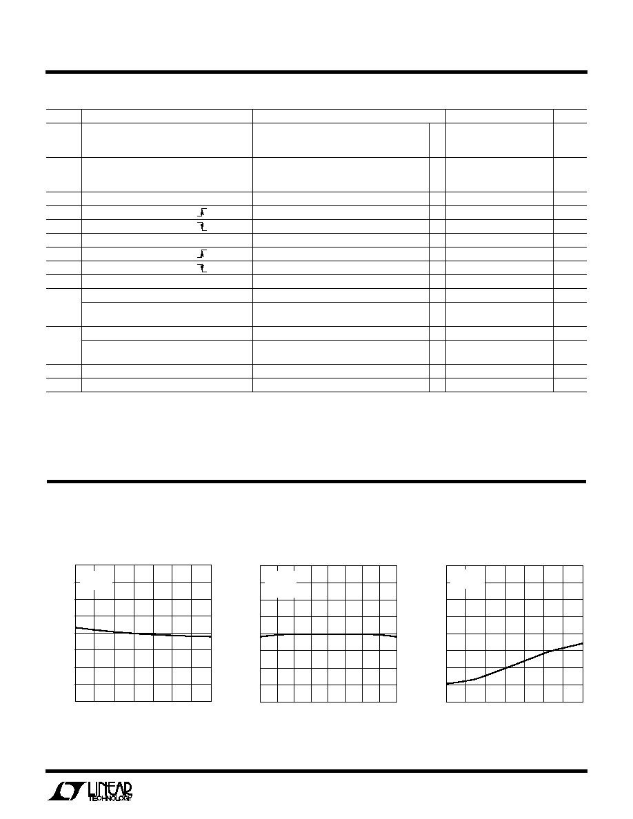
TYPICAL PERFOR
M
A
N
CE CHARACTERISTICS
U
W
TEMPERATURE (°C)
50
OUTPUT CURRENT
(mA)
25
1346A G01
11
10
25
0
50
9
13
12
75
100
125
V
CC
= 5V
V
EE
= 5V
Transmitter Output Current
vs Temperature
OUTPUT VOLTAGE (V)
2.0
OUTPUT CURRENT
(mA)
11
12
2.0
1346A G02
10
9
1.0
0
1.0
13
1.5
0.5
0.5
1.5
T
A
= 25
°
C
V
CC
= 5V
V
EE
= 5V
Transmitter Output Current
vs Output Voltage
Transmitter Output Skew
vs Temperature
TEMPERATURE (°C)
50
TIME (ns)
25
1346A G03
10
5
25
0
50
0
20
15
75
100
125
V
CC
= 5V
V
EE
= 5V
4
LTC1346A
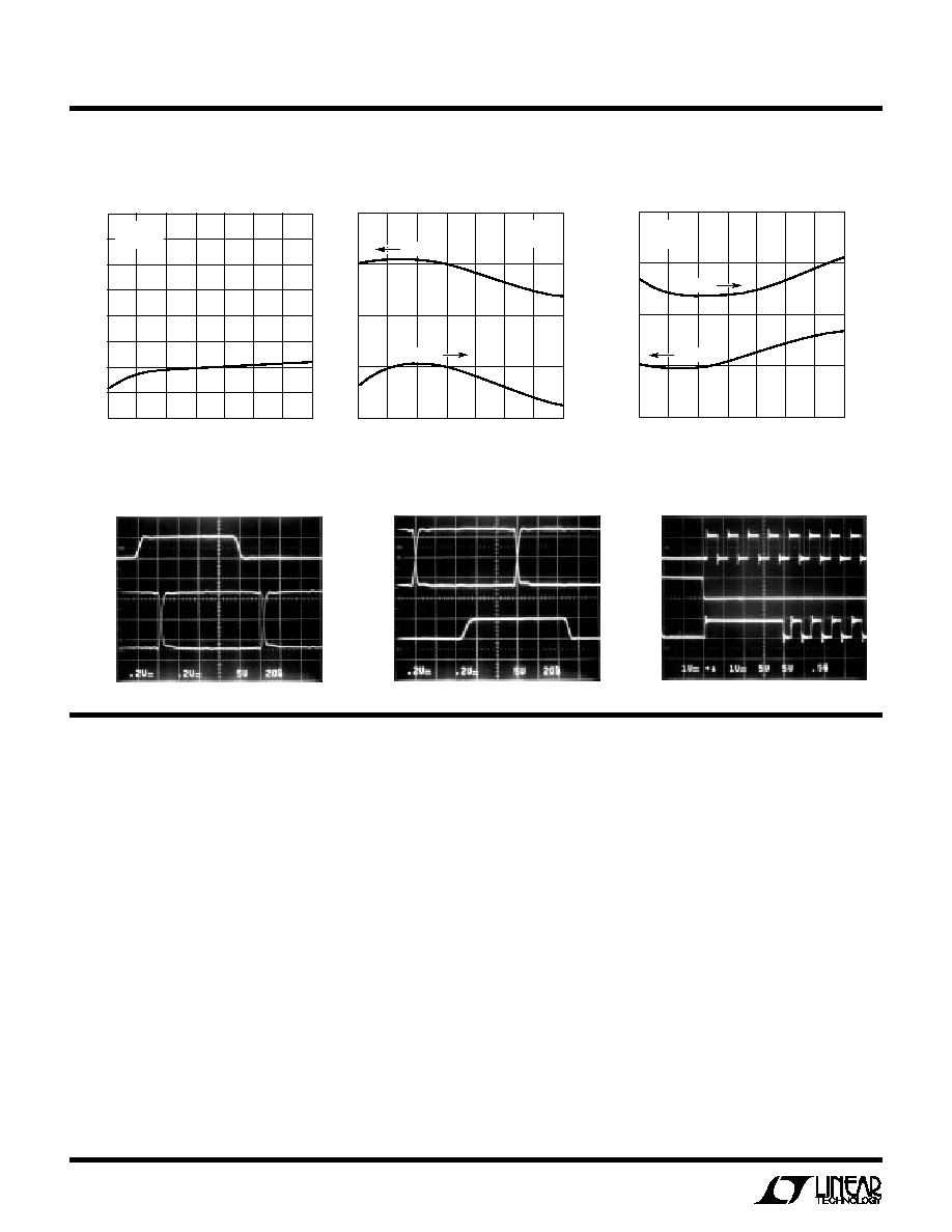
TYPICAL PERFOR
M
A
N
CE CHARACTERISTICS
U
W
B1 (Pin 13): Receiver 1 Inverting Input
A1 (Pin 14): Receiver 1 Noninverting Input
B2 (Pin 15): Receiver 2 Inverting Input
A2 (Pin 16): Receiver 2 Noninverting Input
B3 (Pin 17): Receiver 3 Inverting Input
A3 (Pin 18): Receiver 3 Noninverting Input
Z3 (Pin 19): Transmitter 3 Inverting Output
Y3 (Pin 20): Transmitter 3 Noninverting Output
Z2 (Pin 21): Transmitter 2 Inverting Output
Y2 (Pin 22): Transmitter 2 Noninverting Output
Z1 (Pin 23): Transmitter 1 Inverting Output
Y1 (Pin 24): Transmitter 1 Noninverting Output
V
EE
(Pin 1): Negative Supply, 4.75V
V
EE
5.25V
V
CC
(Pin 2): Positive Supply, 4.75V
V
CC
5.25V
GND (Pin 3): Ground
T1 (Pin 4): Transmitter 1 Input, TTL Compatible
T2 (Pin 5): Transmitter 2 Input, TTL Compatible
T3 (Pin 6): Transmitter 3 Input, TTL Compatible
S1 (Pin 7): Select Input 1, TTL Compatible
S2 (Pin 8): Select Input 2, TTL Compatible
R3 (Pin 9): Receiver 3 Output, TTL Compatible
R2 (Pin 10): Receiver 2 Output, TTL Compatible
R1 (Pin 11): Receiver 1 Output, TTL Compatible
S0 (Pin 12): Select Input 0, TTL Compatible
PI
N
FU
N
CTIO
N
S
U
U
U
INPUT
0.2V/DIV
INPUT
5V/DIV
OUTPUT
0.2V/DIV
1346A G07
1346A G08
1346A G09
INPUT AB
1V/DIV
Receiver Enable from Shutdown
INPUT S0
5V/DIV
OUTPUT
5V/DIV
OUTPUT
5V/DIV
Receiver Output Waveforms
Transmitter Output Waveforms
TEMPERATURE (°C)
50
CURRENT (mA)
CURRENT (mA)
25
1346A G06
35
40
25
0
50
45
25
30
6.0
6.5
7.0
5.0
5.5
75
100
125
LOADED
NO LOAD
V
CC
= 5V
V
EE
= 5V
I
EE
Supply Current vs Temperature
TEMPERATURE (°C)
50
CURRENT (mA)
CURRENT (mA)
25
1346A G05
35
30
25
0
50
25
45
40
6.5
6.0
5.5
7.5
7.0
75
100
125
LOADED
NO LOAD
V
CC
= 5V
V
EE
= 5V
TEMPERATURE (°C)
50
TIME (ns)
25
1346A G04
10
5
25
0
50
0
20
15
75
100
125
V
CC
= 5V
V
EE
= 5V
Receiver t
PLH
t
PHL
vs Temperature
I
CC
Supply Current vs Temperature
5
LTC1346A
FU CTIO TABLES
U
U
Transmitter and Receiver Configuration
S0
S1
S2
DX ON
RX ON
Description
0
0
0
--
1, 2, 3
All RX ON, All DX OFF
1
0
0
--
--
All OFF, Shutdown
0
1
0
1, 2, 3
1, 2
DCE Mode
1
1
0
1, 2, 3
--
DCE Mode, All RX OFF
0
0
1
1, 2
1, 2, 3
DTE Mode
1
0
1
1, 2
--
DTE Mode, All RX OFF
0
1
1
1, 2, 3
1, 2, 3
All ON
1
1
1
1, 2, 3
--
All DX ON, All RX OFF
Transmitter
INPUTS
OUTPUTS
CONFIGURATION S0 S1 S2
T Y1 AND Y2 Z1 AND Z2 Y3 Z3
All OFF
0
0
0
X
Z
Z
Z
Z
Shutdown
1
0
0
X
Z
Z
Z
Z
DCE or All ON
X
1
X
0
0
1
0
1
DCE or All ON
X
1
X
1
1
0
1
0
DTE
X
0
1
0
0
1
Z
Z
DTE
X
0
1
1
1
0
Z
Z
Receiver
INPUTS
OUTPUTS
CONFIGURATION
S0 S1 S2
A B
R1 AND R2
R3
All Rx ON
0
0
0
0.2V
0
0
All Rx ON
0
0
0
0.2V
1
1
Shutdown
1
0
0
X
Z
Z
DCE
0
1
0
0.2V
0
Z
DCE
0
1
0
0.2V
1
Z
Disabled
1
1
0
X
Z
Z
DTE or All ON
0
X
1
0.2V
0
0
DTE or All ON
0
X
1
0.2V
1
1
Disabled
1
X
1
X
Z
Z
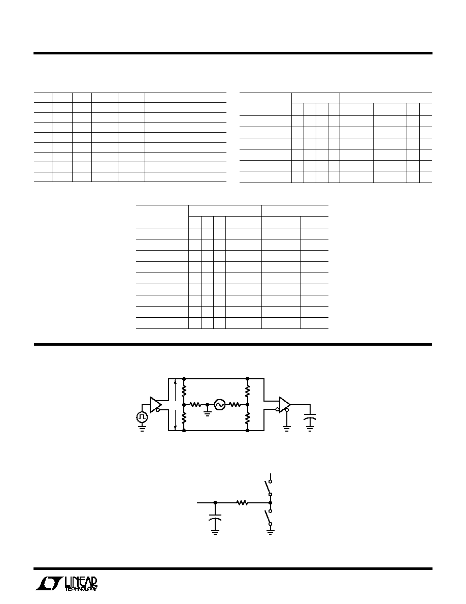
TEST CIRCUITS
C
L
1k
LTC1346A · F02
SW1
SW2
V
CC
RECEIVER
OUTPUT
Figure 2. Receiver Output Enable and Disable Timing Test Load
15pF
S0
R
50
125
Y
Z
Z
Y
T
125
50
50
LTC1346A · F01
50
A
B
V
OD
V
OS
V
OC
= (V
Y
+ V
Z
)/2
Figure 1. V.35 Transmitter/Receiver Test Circuit